Austrian substrate manufacturer AT&S is developing a new generation of miniaturized inductors that can be integrated into multi-layer printed circuit boards. They can enable the production of tiny voltage converters or ultra-thin wireless charging devices. Now researchers at the company are working on perfecting the technology and applying it to more applications. Part of the progress stems from a research and development effort funded by the European Union.
If you want to supply an electric car with electricity or charge your mobile phone wirelessly, you have to rely on electromagnets, which consist of a core made of ferromagnetic material and a coil wound around it. Such magnetic components are ubiquitous in the electrical and electronics industry and the basis for technical progress in many areas. That is why the European Union, as part of its IPCEI initiative (Important Projects of Common European Interest) in the field of microelectronics, has made research into the next generation of such components a priority. AT&S is involved in the project together with more than 30 partners from industry and research.
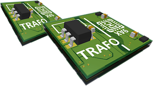
AT&S uses its experience and production capacities in the manufacture of highly complex printed circuit boards to create small electromagnets, which in turn are the basis for integrated components such as inductors or transformers. AT&S engineers are already demonstrating first prototypes, such as a wireless charging device for mobile phones with a printed circuit board just one millimeter thick, at trade fairs.
“The magnetic components that are state of the art today are often wound by hand in low-wage countries. With our know-how from printed circuit board production, we can not only manufacture thinner components but also significantly improve reliability,” says Gerald Weidinger, who heads development at AT&S. Instead of winding an actual wire around an iron core, the windings are realized with the finest of holes around a tiny ring of special magnetic materials that have been embedded in circuit board material.
“We drill through the core of the circuit board inside and outside the ring, the holes are then plated with copper and connected with traces below and above the magnet ring. This creates an embedded electromagnet,” says Weidinger. With this technology, thousands of such elements can be produced in parallel on a single panel. This also enables automated quality control, which contributes to the high reliability of the magnetic elements.
AT&S is currently working on perfecting the technology for customers. By expanding the possible performance ranges, additional applications are being opened. In addition to smaller wireless chargers and more efficient power supply circuits, the technology is also being expanded to make tiny electromagnets in shapes other than toroids. Magnetic layers inside a printed circuit board can also be used to shield sensitive electronic circuits from each other. See www.ats.net.