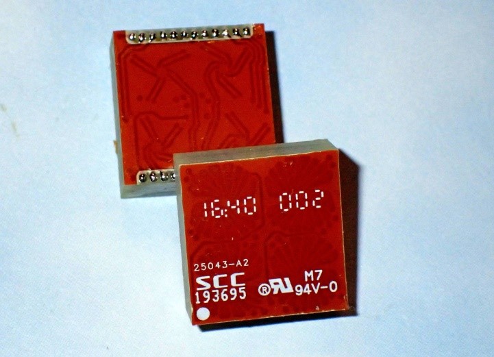
Parts 1 and 2, provided an overview of embedded magnetics construction and presented a design example for a GbE media filter. Performance data showed that the embedded magnetic devices are highly consistent. Part 3 looks at the material used in the PCB construction and summarized reliability data. Figure 1 shows an example of a surface mount GbE media filter fabricated with embedded magnetic technology.
During reliability testing, parts are stressed under heat and humidity conditions to try and accelerate failures and identify weak spots in the design. Parts will undergo thermal cycling and be cooked in an autoclave under high pressure and humidity to heighten internal stresses. These tests can accelerate deterioration and provide an indication of how the part will hold up under normal operating conditions. Vibration and mechanical shock test the mechanical integrity of the package. With an embedded magnetic design, the conductors are laminated and plated onto the FR-4 substrate and it is essentially a solid-state construction. There are not free -floating wires or internal solder joints that can be become brittle and fail under thermal stress, vibration and mechanical shock. So in this case, the parts are surface mounted onto a test coupon and we are really testing the integrity of the solder balls on the I/O pads.
The GbE media filters are generally deployed on personal computers and LAN networking equipment. The working environment in an office or data center will usually be temperature controlled and have an operating range between 0C to 70C. If utilized in a security camera or wireless access node, then there is the potential for outdoor deployment. Outside deployments can experience temperatures ranging from -40C to +85C. Table 1 summarizes the reliability testing that was used to stress the embedded magnetic media filters. For this case, the parts were stressed tested for use in an indoor environment. Samples size was 20 units and the pass criteria was determined by testing for opens, shorts and the Open Circuit Inductance (OCL ≥ 350 uH) of the transformers on all 4 channels. Parts were also tested for Hipot (voltage breakdown) before and after undergoing the stress testing.
Table 1, Summary of Reliability Testing
| Items | Condition | Passing Units |
| High Temperature Storage Life(HTSL) | 105℃+2/-0, 1000h | 20/20 |
| Thermal Shock and Humidity/Temperature Cycling | Step1:-65℃ ~ 125℃/15min, 25cycle. Step2:-10℃~65℃, 80%~98%RH, 10cycle (240h). | 20/20 |
| Temperature Cycling | Step1:105℃/6h baking. Step2:-15C~85C, 5℃/min rate, dwell time 10min, 500 cycle (400hrs) | 20/20 |
| Random Vibration and Mechanical shock | Step1:Random Vibration 20~500Hz, PSD 0.02g2/Hz, RMS 3. 10g, 15min/axial, XYZ axial. Step2:Mechanical Shock 50g/11ms, 3cycle/direction, XYZ axial. | 20/20 |
| Hipot Test | Step1:1500Vrms, 1 min | 20/20 |
Hipot is a safety issue and warrants special consideration. It is a voltage stress test and provides a metric of the transformer’s ability to isolate the end node/user from a voltage surge or lighting strike that may hit the transmission cable. Wire wound GbE transformers are wound with 32AWG magnet wires that is coated with about 0.04 mm of polyimide insulation. This is sufficient to provide 1500Vrms of isolation, as long as the wire is not kicked or scratched during fabrication. PCB materials are also good dielectric insulators. FR-4 laminates are commonly rated at 29kV/mm (750V/mil), and will generally hold against breakdown as long as there is ≥ 0.08 mm (3 mils) separation between conductors. Similarly, liquid image solder mask has breakdown voltages rating of 19.5kV/mm (500V/mm). The issue with solder mask is that it is applied with a screen printing process and there can be small pin-holes in the covering, due to micro bubbles or micro-cracks. During hipot testing, the air around the exposed I/O pads will become ionized and an ion cloud can form above the device surface. In that case, breakdown can occur vertically through a surface defect to the underlying trace, rather than between adjacent traces that reside under the insulating layer. To prevent this from happening, 2 or more solder mask layers should be applied to cover any micro defects in the first layer. An alternative is to use a dry film or polyimide cover lay material, which are homogeneous and have dielectric breakdown voltages of 3000kV/mil (117kV/mm). The cover-lay provides higher breakdown voltages; however the material and process cost is higher than applying solder mask. The GbE media filters in figure one have a polyimide cover-lay and exhibit breakdown voltages exceed 2.5 kVrms.
To summarize this 3 part series, embedded magnetics are essentially fabricated as you would a printed circuit boards and exhibit reliability consistent with most PCBs. Devices are fabricated in a batch process using automated manufacturing technology. The labor content is a small fraction of what is used to fabricate wire-wound magnetics. The fact that the windings are defined by photolithography provides a high degree of consistency from device to device. This is particularly useful for RF applications, where the high frequency performance can be modeled and optimized before a design is committed to fabrication.

About the Author: Jim Quilici develops magnetic components for Shennan Circuits (www.scc.com.cn). He holds an MSEE from University of Arizona and has over 30 years of experience in developing magnetics and microelectronics. He has been awarded 9 patents associated with PCB magnetics. Jim also is a part-time lecturer at California State University Sacramento where he teaches courses on Network Analysis and Microelectronics. He can be reached at jim.quilici@scc-america.com.