What is EnaChip up to? That’s an important question for design engineers of power electronics systems to ask these days. By coating specialized magnetic alloys directly onto semiconductor substrates — and other innovations, the semiconductor microdevice company is bringing disruptive technology to the forefront as it works to commercialize a breakthrough wafer level magnetic technology platform capable of enabling new classes of electronic products. We asked Trifon Liakopoulos, co-founder and CEO of EnaChip, to bring us up to date.
First, it is important to understand a little background about the company’s core technology — single mask thin film magnetic core laminations for high performance wafer level magnetics. The concept has far-reaching implication, notably, enabling affordable integrated power for every semiconductor chip in a node-agnostic system that is capable of providing magnetic functionality processed on virtually any substrate from any foundry including active ICs.
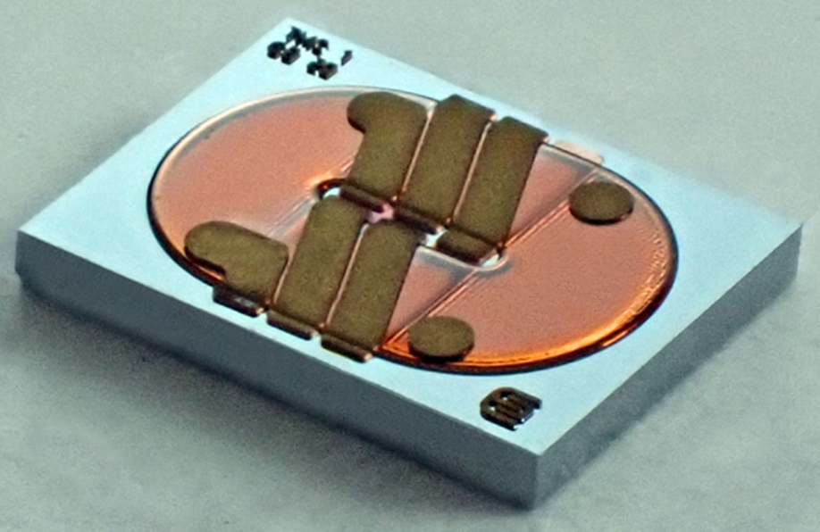
EnaChip’s transformative technology is known as Trifecta. Founded on material innovation, the company focuses on three key areas — cutting edge performance magnetics, manufacturing & packaging innovation and artificial intelligence-enhanced design library modules. Key factors include proprietary wafer level magnetic materials that enable high operating frequencies up to 50 MHz, high resistivity films that require fewer core laminations, high magnetic saturation and innovative cost-effective fabrication methods. The system is based on photoresist electroplating of copper windings and single-mask sequentially plated core laminations.
Standard practice in the semiconductor industry today is to use sputtered laminated cores, building them layer by layer in a process where 20 to 40 layers might take 20 hours of process time. In comparison, EnaChip’s continuously electroplated laminated cores can accomplish the equivalent process in a single layer. The simpler process means an ultra-fast deposition time that can be 100 times faster, leading to a significant reduction in manufacturing expenses.
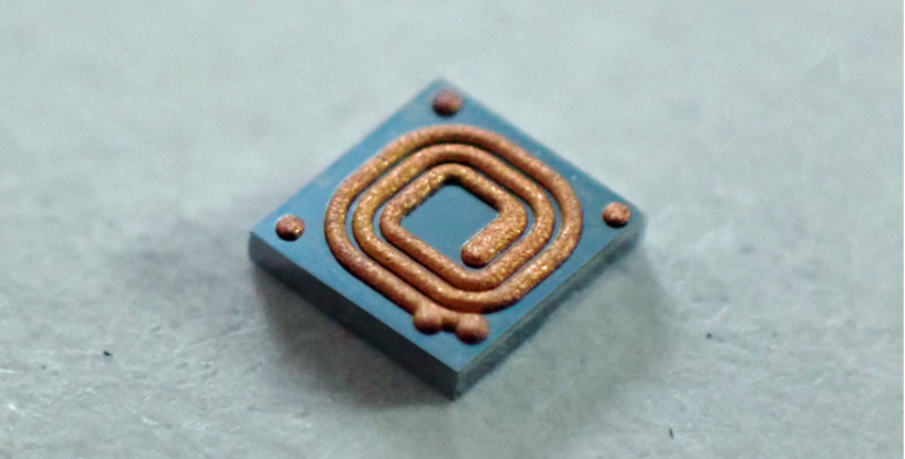
Tunable for target applications, the company’s proprietary alloys essentially provide programmable material intelligence, enabling seamless power design optimization on any chip. Its wafer level magnetics can meet the performance of discrete components in dramatically less volume – as much as 276 times smaller, says the company.

“We are actively fund-raising now, and working with strategic partners and investors. We are operating in dual mode – licensing, and developing our own products. We have a pilot capability to develop prototype devices and presently are working with several companies in product development, including a large passives manufacturer and some major OEM’s”
“I think the most important aspects of our platform are that we have developed unique magnetic alloys and unique microfabrication processes. Our material has properties of high saturation, high current and high inductance. We can program it for specific applications. Applications that we are currently focused on are power management ICs, isolated power, and voltage regulators. Additionally, our wafer level magnetics technology platform can be extended to on-chip magnetic sensors, micro-relays and actuators with applications extending from aerospace and navigation to smart health microdevices.”
Located in Rocky Hill, New Jersey near Princeton, EnaChip presently has a staff of 10 people. Matt Wilkowski, vice president of engineering, leads the technology efforts spearheaded by two talented engineers – Kamyar Ahmadi, director of materials engineering, and Mo Khodadadi, director of magnetics and processing. The company began operations in 2018 as a magnetic materials startup. In 2021, it raised $7.1M in venture funding to pursue its development efforts and growth opportunities.
Current roadmap focus is on power management applications such as power management ICs and DC/DC voltage regulators. Other target applications in power management include 3D-HI & IVR, LED drivers, wireless charging. Signal conditioning is seen as another key area with application in high-speed data transfer, filters and tuners.
With full-stack capabilities from design-to-substrate, a key activity for the company is applying its capabilities to help companies launch high performance, power efficient, smaller electronic products with higher margins. It offers customized devices using its wafer-level magnetic technology platform that enables the manufacturing of high-efficiency inductors and transformers for use in power-management integrated systems, signal isolation sensitive circuit components where data integrity is critical, magnetic sensors for niche navigation and guidance applications, and magnetic actuators such as those used in medical point-of-care devices. For more info, see www.enachip.com