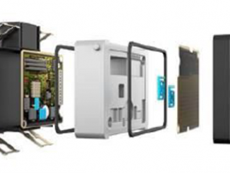
Magnetic components are widely used in conjunction with semiconductor devices. For telecommunication applications, transformers couple signals into transmission lines and antennas. They provide impedance matching, level shifting, voltage isolation and common mode filtering. In power applications, transformers and inductors are used for energy storage, level shifting, isolation and noise filtering. Over decades, the semiconductor industry has made continual improvements in reliability, to the point where failure rates today are in the 1 part per million and are now trending towards parts per billion. In contrast, magnetic components have lagged behind their semiconductor counterparts and often exhibit failure rates in the range of 50 to 1000 ppm. This fact often positions the magnetics as the “weak link” in system reliability.
When fabricating the small transformers and inductors used in data communications, it is often difficult to employ automatic winding. A large percentage of magnetic components coming out of Southeast Asia are still manually wound. Such high level of manual content introduces failures in the form of shorts due to nicked wire insulation and opens due to kinked wires and cold solder joints. Even when automatic winding is employed, there is still a considerable amount of manual content required to dress, terminate and solder the wires to the package pins. Manual construction can also result in relatively large performance variance from device-to-device.
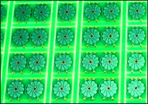
Embedded magnetics advances the reliability and consistency of magnetic components. Figure 1 shows an example of embedded magnetic transformers that have been step and repeated on a PCB panel. Figure 2 depicts a cross section.
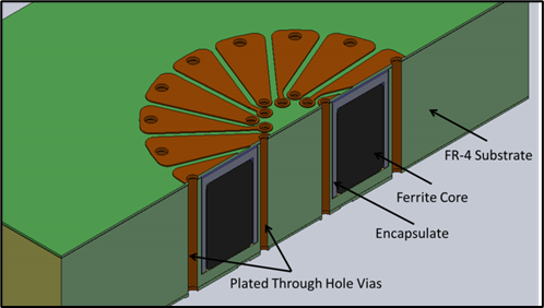
In this construction, cavities are routed into a FR-4 (fiberglass) substrate and ferrites cores are inserted and encapsulated with a low shrink epoxy. After embedding the ferrite cores, the fabrication follows standard PCB processes. Copper foil is laminated to the top and bottom surfaces and interconnecting vias are drilled and plated between the layers. The inductive windings are then imaged and etched onto the top and bottom surfaces. Using photolithography to define the windings assures accurate placement and highly consistent performance. Secondary parameters; like winding resistance, inter-winding capacitance, leakage inductance and voltage isolation, can be managed by controlling the width and separation between the conductors. The end product is essentially a solid state device and has reliability consistent with a PCB. Table 1 summarizes the features and benefits
Table 1, Features and Benefits of Embedded Magnetics
| Features | Benefits |
| Fabricated on a Printed Circuit Board line | Utilizes automated and batch processes Portable process that leverages existing capital equipment investments Low labor content Reliability consistent with PCB technology |
| Windings are defined by photolithography | Highly consistent, performance defined by circuit artwork RF testing can be done on a lot sample basis Conductors can be shaped and spaced to control resistance, inductance, capacitance and voltage isolation Performance can be accurately modeled and optimized with an RF simulator |
| Vertical Integration | Multiple transformers and inductors can be arrayed and stacked to minimize the device footprint The magnetic device is essentially a PCB upon which other passive and active surface mount devices can be placed |
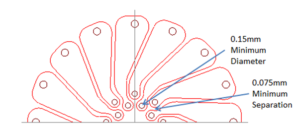
Of course, among these benefits there are also limitations. The primary being that embedded magnetics generally requires the use of larger ferrite core sizes, compared to wire-wound construction. Figure 3 shows a section of the artwork for a transformer. Inductance is determined by the ferrite material properties and the number of windings that are applied. The number of windings is limited by the “window area” of the core. Placement of inter-connecting vias in the window-area requires certain design rules to be followed for manufacturability. Via hole diameters are determined by the aspect ratio (panel thickness/drill diameter) and what can be plated in volume production. Generally, most PCB manufactures can drill via diameters as small as 0.15mm (6 mils) and plate aspect ratios ≥ 15:1. Additionally, the via holes should have a minimum annular ring of 0.075mm (3 mils). Line separation is another factor that impacts manufacturability and voltage isolation. Consequently, larger cores are required to provide enough area for the center via array. With conventional wound wires, one can always cram smaller gauge wires into the window are compared printed circuit vias. Consequently, Embedded Magnetics will require a core that is 20% to 50% larger than a wire wound implementation. While the price difference is small, the bigger drawback is when there are constraints on size.
Additionally, core height determines the required panel thickness and is also a limitation. Most PCB manufacturers can process panels up to 7 mm (0. 275”) thickness. Thicker panels are possible, yet usually require the manufacturer to re-configuration the conveyors on their etching system. While possible, most manufactures are reluctant to re-configuring their etching lines for a specific job.
Even with these constraints, it is still possible to address a wide variety of Telecommunication, RF and Power applications. Part 2 of this series will provide an overview of an Ethernet media filter realized with this technology. Part 3 will then summarize reliability testing and look at particular details associated with voltage isolation.

About the Author: Jim Quilici develops PCB magnetics for Shennan Circuits (www.scc.com.cn). He holds an MSEE from University of Arizona and has over 30 years of experience in developing magnetics and microelectronics. He has been awarded 9 patents associated with PCB magnetics. Jim also is a part-time lecturer at California State University Sacramento where he teaches courses on Network Analysis and Microelectronics. He can be reached at jim.quilici@scc-america.com.