By Jim Quilici, SCC America
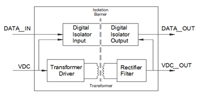
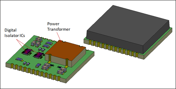
Battery stacks used in automotive and energy storage systems can have voltages ranging from 400 to over 1000 volts. These systems require continual monitoring and management to maintain the integrity of each battery. Voltage and temperature sensors on the battery stack have a floating reference potential, which can vary depending on where the sensors are located on the stack. Data channels from the stack continually feed data to a controller which manages the battery status and integrity. Often, these data channels cross need to cross a high voltage isolation barrier before connecting to the control circuitry that is referenced to either chassis or earth ground. The isolation barrier is required to protect the controller circuitry, which often runs at +5V volt levels or lower. Digital isolators are commonly used to move data and control signals between the stack and controller. Digital isolators have been around for over a decade and utilize capacitive coupling to isolate input voltages from the output. Silicon Oxide is quite a good insulator and it is practical for implementing small capacitors within an integrated circuit that have breakdown voltages exceeding 2kV. This is fine for passing logic level signals across the isolation barrier. However, power still needs to cross the isolation barrier to bias the output circuitry on the high side. SiO2 capacitors are too small for this function and an isolated switch mode power converter is required. The power converter is built around a transformer, which translates voltage levels and establishes the isolation barrier. Figure 1 depicts gate drive circuity that uses digital isolators for the control channels and an auxiliary power converter to deliver supply voltages to the high side. Historically, the high isolation DC/DC converter has been implemented as a discrete component independent of the digital isolator function. However, in recent years the trend has been to integrate the DC/DC converter next to the isolators as a System in a Package (SIP). The benefit of this integration is convenience and a small application footprint.
Traditionally, transformers have been constructed by winding wire around a magnetic core or bobbin. For high voltage isolation, this often requires using double insulated “reinforced” wire, which is difficult to work with. SIP packaging also requires transformers with a low profile and small footprint. For such small transformers, the added insulation makes the wire especially difficult to wind. In addition, the
wire gauges can be in the range of 28 AWG (6 mil diameter) to 32 gauges (4 mil diameter). It is difficult to strip the insulation off such small wires so that they may be soldered or bonded onto the system circuit. An Embedded Magnetics construction provides a robust alternative to winding wire around a core. Rather than building transformers one at a time, small power transformer can be fabricated on a PCB production line using batch processes.
Embedded Magnetics Construction
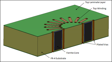
To begin, a cavity is routed into a FR-4 substrate, to receive the magnetic core. A ferrite toroid is dropped into the cavity and encapsulated with a low shrink epoxy. Some DC/DC converter architectures, like the popular Flyback converter, require that the core first be gapped. Once the cores are in place and encapsulated, the panel is planarized to remove any excess epoxy and prepare the panel for laminating printed circuit layers. At this point the panel follows standard PCB processing steps. Copper foil is laminated to the substrate with thin sheets of pre-preg, which is a woven fiberglass impregnated with partially cured epoxy. Under the pressure and temperature of a laminating press, the pre-preg epoxy flows and bonds the copper foil to the substrate. Winding layers are applied using standard drilling, plating, imaging and etching processes. PCBs can be processed in large panel formats. For the small devices that might reside in a SIP package, a standard 610 x 457mm panel may contain over 1000 devices. So every time a technician handles the panel and puts it in plating or etching tank, they are handling a batch of 1000 devices. These batch processes provides much efficiency, compared to the traditional method of winding wires on individual cores, one at a time. Figure 2 shows a cut-way view of an embedded magnetic device.
Design Example
As an example, we can look at a 3W power transformer that Shennan Circuits developed for a digital isolator SIP. As depicted in Figure 1, the transformer is part of a DC/DC converter that provides supply voltages to the high voltage side of the isolation barrier. In this particular application, the transformer is required to have a 5:6 winding ratio and isolation barrier that can exceed 7.5kV AC. Additionally, the transformer is packaged in a SIP module that is over-molded with epoxy and requires that the transformer have a low profile of ≤ 2.2mm. The over-molded epoxy essentially covers the I/O pads on the transformer so that the clearance/creepage requirements apply to the exposed metal on the I/O of the SIP package and not the transformer package.
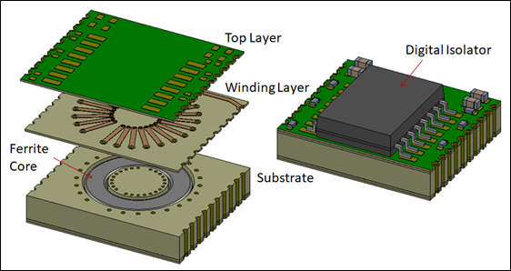
Figure 3 depicts the transformer implemented in a SIP package. The transformer and bias components are first surface mounted to the substrate, prior to die attaching and wire bonding the digital isolator ICs. Transfer molding is then used to cover the whole assembly with epoxy.
PCB laminates are quite good insulators. General purpose FR-4 has a breakdown voltage of 20kV/mm while grades designed for high voltage applications have breakdown voltages exceeding 45kV/mm.
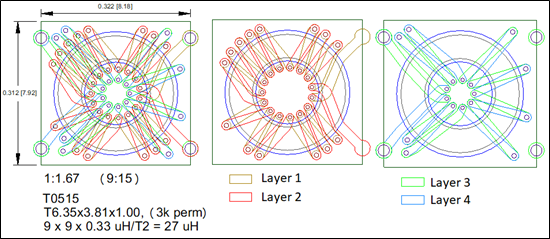
For this design, a Manganese Zinc (MnZn) ferrite material was selected with a relative permeability of 3000. A T6.5×1.5×1.0 size core was selected, which has an inductance factor (AL) of 0.33 uH/T2. The power converter circuit requires that the transformer provide an inductance of > 27uH and a 1:1.67 winding ratio to provide a voltage step-up between the primary and secondary windings. Considering the AL factor, it was calculated that there should be 9 on the primary side and 15 on the secondary side. There are a few basic configurations that can be used for implementing the printed windings. As shown in Figure 4, they can be labeled Bifilar, Sector or Overlapping. Each has their own benefits and drawbacks. Bifilar and Sector windings can be implemented with two copper layers while the overlapped windings require 4. For the 7.5kV transformer, an over-lapping winding was selected, primarily for the properties of high voltage isolation and low leakage inductance.
Besides inductance, transformers have the secondary parameters of winding resistance (RDC), leakage inductance (LL) and inter-winding capacitance (Cww). RDC and LL are loss mechanisms and should be kept low to maximize efficiency. Cww provides a conduit for switching noise to cross from the primary to secondary winding and also should be kept low. In Figure 3, the windings are drawn with consistent width conductors. The designer has the option to also flare and shape the windings to manage these secondary properties.
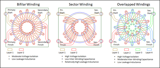
Figure 5 shows the artwork for the 27uH transformer. The secondary windings have 15 turns and are implemented on the inner layers; Layer 1 and Layer 2. The conductor widths are 0.4 mm wide and separated by 0.13 mm. Between the layers, the windings are connected with 0.25 mm plated-through- hole (PTH) vias. The primary winding has 9 turns and is implemented on the outer layers; Layer 3 and Layer 4. The vertical via barrels between layer 3 and layer 4 are placed 0.4 mm away from the copper conductors on the inner layers, a distance which provides ≥ 18kV of isolation.
For the overlapped windings, we rely on the pre-preg laminate layers to provide the isolation between the primary and secondary windings. For this design, an automotive grade pre-preg [2] was selected. This material is a lead-free and has a voltage breakdown rating ≥ 45kV/mm. The laminate sheets come in different thicknesses [3]. To provide ≥7.5kV of isolation, 3 sheets of pre-preg with a 1080 fiberglass weave is used. This stacks up to a thickness of 0.183 mm, which corresponds to an 8.2kV breakdown voltage. On the top and bottom surfaces, a polyimide cover-lay [4] was applied to cover the conductors. The polyimide film and bond-ply adhesive film are each 0.25 mm thick. Polyimide has a breakdown voltage of ≥137kV/mm and the 0.25 mm film thickness provides >3.5kV. Since the transformer is being over-molded in the SIP package, the polyimide cover-lay does not necessarily need to meet the full 7.5kV AC breakdown requirement.
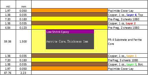
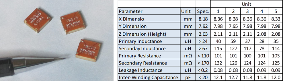
Figure 7 shows finished transformers and summarize the specifications and test results for 5 parts. On average, the primary inductances came in much higher than the 27uH spec. Winding resistance on the primary side was measured at 100mΩ, which is low for a transformer of this size and good for low loss and high efficiency operation.
Since the clearance distance was below IEC 62368-1 specifications, Hipot testing was done while the transformers were submerged in a bath of insulating oil. A lot sample of 10 devices was tested and all passed 7.5kV AC and 10KV DC for 60 seconds without voltage breakdown between the primary and secondary windings. As mentioned earlier, once assembled onto the SIP substrate, the assembly is over-molded with epoxy. The final assembly also passes Hipot at 7.5kV AC and 10kV DC.
Of course an alternate construction is to combine the embedded transformer with PCB substrate. Figure 8 shows an assembly where the embedded transformer becomes the substrate upon which a digital isolator in a DIP package is mounted on the top surface along with biasing resistors and filter capacitors. Combining the transformer with the PCB substrate brings additional cost savings and can reduce the SIP module footprint.
Conclusion
A design example has been provided for integrating a low profile power transformer into a SIP package. The transformer was implemented using embedded magnetic construction and fabricated on a standard PCB line. The transformer was implemented in a 4 layer design, where the breakdown voltage properties of the laminates are critical for maintaining voltage isolation. FR-4 Laminate and coverlay materials were selected to successfully achieve a Hipot breakdown voltage exceeding 7.5kV AC. Given that the line widths and separation between the transformer windings are defined by photolithography the electrical performance is highly consistent between individual devices and fabrication lots. With such consistency, it is practical to do Hipot testing on a lot sample basis and not necessary to test each device in production.
References:
- IEC 62368-1 Standard Compliance Guide, International Electro-Technical Commission, December 20, 2020
- S1000-2M Data Sheet, rev1, ShengYi Technologies Inc., February 2017
- Pre-preg thickness Chart, https://www.4pcb.com/media/prepreg-thickness-chart.pdf
- Pyralux FR Coverlay & Bond Ply Data Sheet, Dupont Corporation, https://www.dupont.com/products/pyralux-fr.html, October 2022
- Embedded High Voltage Transformer Components and Methods, United States Patent, US10522,279 B2, December 31, 2019
Author Biography

Jim Quilici develops PCB magnetics for Shennan Circuits (www.scc.com.cn). He holds an MSEE from the University of Arizona and has over 30 years’ experience developing microelectronics and semiconductor circuits. He has been awarded 9 patents associated with embedded magnetics. Jim is also a part-time lecturer at California State University Sacramento where he teaches courses on Network Analysis and Microelectronics. Jim is based in Northern California and can be reached at jim.quilici@SCC- America .com