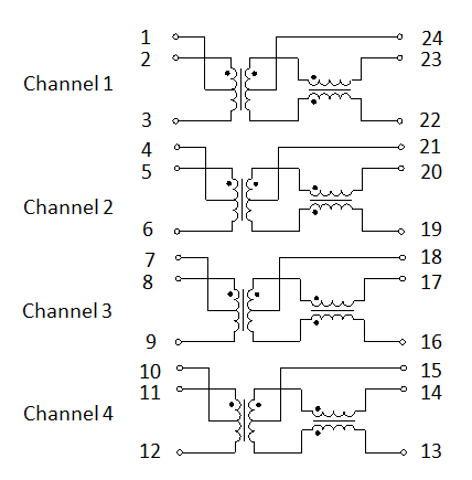
Part 1 of this series provided an overview of embedded magnetic construction. Part 2 looks at the implementation of an Ethernet media filter with the embedded technology. Ethernet has been the leading conduit for Local Area Networks (LANs) since the late 1980s. It has evolved from 10 Mb/s data rates exceeding 100 Gb/s1. Readers familiar with the technology know that behind every wire-line Ethernet port reside 8 or more transformers. Their function is to couple the signal from the transceiver IC to the twisted pair cable and filter noise. Figure 1 shows a typical schematic for a Gigabit Ethernet (GbE) media filer. GbE is the data speed available on most laptops and personal computers.
Historically, the transformers in these modules have been hand wound and hand soldered into their respective packages. This is amazing when one considers that over 500,000 Ethernet ports are shipped each year. In recent years, automatic winding technology has advanced to the point where many of the transformers in the lower speed Ethernet applications can be wound automatically. Even still, dressing the wires and soldering them into the packaging is still mostly done manually. For higher speed applications, like 5GbE and 10GbE, the windings are often implemented using twisted wire to carefully control the differential impedance of the wire. Twisted wire and the small core sizes add complexity that defies automatic winding.
Embedded magnetics eliminates most of the manual content. Devices are fabricated with automatic and batch processes. They are arrayed in a PCB panel format, so every time a technician handles a panel, they are touching hundreds of devices. Given that the windings and interconnects are implemented through photolithography, reliability issues associated with wire insulation and solder are eliminated. Also, the RF performance characteristics are defined by design and can be tested on a sample lot basis. Testing merely requires probing with and LCR meter to verify inductance, winding resistance and detect opens and shorts. This can be done very effectively with a flying probe or bed-of-nails tester, which is equipment commonly found on a PCB fabrication line.
The schematic shows 4 data channels, each channel has a Common Mode Choke (CMC) and Isolation transformer. The isolation transformers are usually implemented with high permeability (≥ 5000) Manganese Zinc (MnZn) ferrite material. The CMCs provide noise filtering and are generally implemented with lower permeability (800 to 1500) Nickle Zinc (NiZn) material. Those familiar with these materials know that the permeability can be diminished when pressure forces are applied. When the ferrites are embedded into the FR-4 substrate panel, they are encapsulated with a low shrink epoxy to minimize stress on the ferrites. The top surface of the panel is then planarized (sanded flat) to provide a flat surface for lamination. After the ferrites cores are embedded into the panel, the subsequent steps follow standard PCB processes. Copper foil is laminated to the top and bottom surface of the panel. Lamination pressures can exceed 150 PSI, however as long as the cores are encapsulated, they will be protected from the lamination pressure and there will not hold residual pressure once the panels are removed from the press. Once copper foil is applied, interconnecting vias are drilled and plated. Photolithography is then used to image and etch windings on the top and bottom surfaces. Solder mask or polyimide cover-lay is applied to provide voltage isolation between the conductive windings.
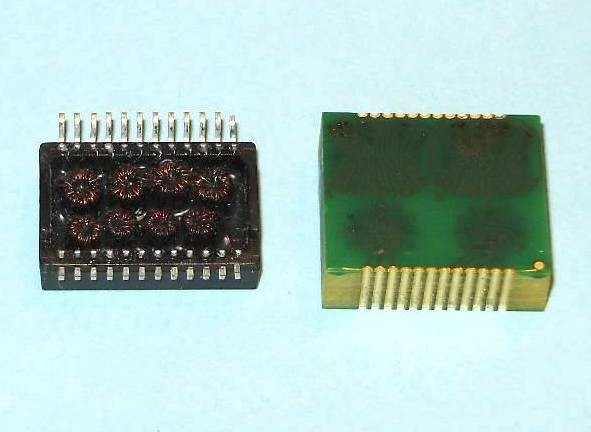
Figure 2 compares GbE media filters that are hand wound and fabricated with embedded magnetics. As noted in part 1, embedded magnetics generally requires the use of larger core elements, compared to the hand wound construction. A close look at the photo gives one a sense of the difference in core sizes. In this particular implementation, the transformers are implemented on a 6.35 mm OD cores. The cores are too large to allow all 8 transformers to fit within two PCB layers. To match the footprint of the conventional wire-wound design, two embedded magnetic boards are laminated together, each layer containing 2 of the 4 channels.
Most of the spectral energy within the GbE signal lies in the range of 60MHz and 125 MHz. Two key performance metrics are insertion loss (SDD12) and return loss (SDD22). Insertion loss is a measure of signal attenuation and return loss is a measure of impedance matching. Mismatch between the cable and the termination at the IC can result in noise due to signal reflections.
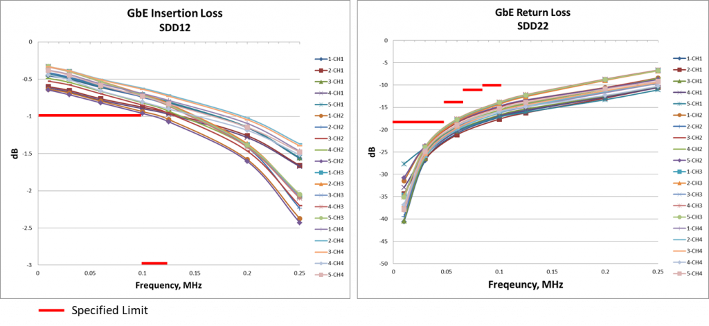
Figure 3, Composite RF Performance Curves
Figure 3 shows composite RF performance curves for 5 devices, 4 channels each. The performance limits are based on the IEEE 802.3ab system specification. In both cases, each of the 4 channel has a unique characteristic and most of the variation is due to the difference in circuit layout for each channel. From part-to-part, the performance clusters around the channel characteristics. The return loss is a key parameter for passing radiated and conducted emissions testing. The performance shows a much tighter distribution compared to an implementation where the transformers are hand wound and soldered into place. In both cases, the performance matches the performance of hand wound devices, however with much less variance.
In part 3 of this series, reliability data will be summarized for the embedded magnetic design. Additionally, the PCB material properties and voltage isolation will be discussed.

About the Author: Jim Quilici develops magnetic components for Shennan Circuits (www.scc.com.cn). He holds an MSEE from University of Arizona and has over 30 years of experience in developing magnetics and microelectronics. He has been awarded 9 patents associated with PCB magnetics. Jim also is a part-time lecturer at California State University Sacramento where he teaches courses on Network Analysis and Microelectronics. He can be reached at jim.quilici@scc-america.com.