Information technologies will be responsible for about 20% of electricity consumption worldwide by 2025, which urgently requires the development of new types of greener nanoelectronic devices. Spintronics, making use of not only the charge of electrons but also of its intrinsic angular momentum (its spin) is an emerging technology that can overcome some of these challenges, thanks to its non-volatility character, full compatibility with CMOS (complementary metal-oxide-semiconductor), low and fast write/reading processes, and high endurance.
However, as nanoelectronic devices move towards denser forms exploiting three dimensions, new mechanisms to efficiently interconnect functional planes become necessary. The shift to 3D devices should enable ultra-highly dense storage and memory devices, but their realization brings huge challenges, from their fabrication to their interconnection or effective heat dissipation.
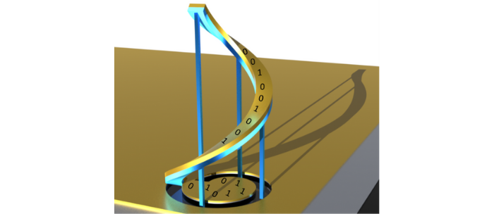
In a work recently published in ACS Nano, an international team led by Luka Skoric (from the Cavendish Laboratory of the University of Cambridge in UK), and Amalio Fernández-Pacheco (from the Institute of Nanoscience & Materials of Aragon in Spain), propose and demonstrate for the first time a new concept for the transfer of magnetic data in three dimensions based on geometrical effects for the interconnection of functional spintronic planes. Unlike traditional spintronic devices which use pulses of current to move magnetic bits, this mechanism exploits instead large thickness gradients, which promote the spontaneous motion of bits without the need to apply any external stimuli. The magnetic data in these devices are encoded as domain walls that “auto-move” without external stimuli along nanowires with spiral shape.

“This work proposes and demonstrates for the first time a new concept for the transfer of magnetic data in three dimensions based on geometrical effects” says Luka Skoric from the University of Cambridge and lead author of the publication. “Until now, the motion of magnetic bits in spintronic devices such as the racetrack memory has been typically based on applying external inputs, typically electrical current pulses. The scalability of racetrack devices to three dimensions is very appealing for future technologies, but brings great challenges regarding their fabrication and heat dissipation during operation. The automotion of domain walls across the devices demonstrated here is a robust and flexible way to move bits in 3D”.
You can think about this effect as a “magnetic nano-elevator which transmits information between spintronic planes” says Amalio Fernández-Pacheco, senior lead author of the publication. “Once the domain walls are introduced into the 3D nanowire devices, they move by themselves without the need to apply any external input as normally required, namely magnetic fields, voltages or electrical currents. The geometry of the devices does it all.”
The devices were fabricated at the University of Cambridge by a combination of state-of-the art nanoscale 3D printing and thermal evaporation, and consist of 3D spiral structures of several microns in length and a few tens of nanometre in width and thickness. After their fabrication, they were investigated at the ALBA Synchrotron and the Synchrotron SOLEIL (France), where X-ray microscopy techniques were employed to directly observe the automotion of domain walls. Experimental studies were complemented by employing micromagnetic simulations developed at the University of Vienna.
The automotion of domain walls had been previously observed in planar spintronic devices due to several mechanisms, from curvature to width gradients, as well as dipolar interactions. Here, for the first time and thanks to state-of-the-art nanoscale 3D printing, it has become possible to leverage 3D geometrical effects for this purpose. This work opens a new route for the integration of future 3D spintronics devices in microchips. It also opens new avenues for the development of highly interconnected neuromorphic spintronic devices.

Experiments at the ALBA Synchrotron
Synchrotron radiation techniques were key for this study in order to characterize the magnetic structures and confirm their functioning, since standard characterization techniques are not able to cope with the complicated 3D geometry. In particular, Photoemission Electron Microscopy with X-ray circular magnetic dichroism contrast (XMCD-PEEM) images obtained from the shadow of the spiral objects gave the researchers the possibility to monitor the magnetic domain wall location during their experiments. Furthermore, the measurements required a unique PEEM sample holder with a two-dimensional vector magnet designed at ALBA in order to precisely nucleate and release the domain wall before automotion.
“We are not only pleased by this fascinating scientific achievement, but also to see how our efforts in preparing the best possible instrumentation are paying off for our users. “ says Michael Foerster, beamline scientist at the PEEM end station of the CIRCE beamline in ALBA, “ and we want to make this also an opportunity to thank all the ALBA staff who is supporting us and the users on a daily basis. These developments were a joint project between different divisions and had many people involved: Technicians, Engineers and experts in magnet design.”
The international team responsible for this work is formed by members from the University of Cambridge and the University of Glasgow (UK), the Spanish National Research Council-CSIC (Spain), the Max Plank Institute for Chemical Physics of Solids in Dresden (Germany), the University of Vienna (Austria), the University of Oviedo and the University of Zaragoza (Spain), the Synchrotron SOLEIL (France) and the ALBA Synchrotron.


