Having already built an accelerometer embedded into a chip and issued its first IP license, British company Nanusens plans to roll out its MEMS technology to other sensors including magnetometers, gyroscopes, pressure sensors and microphones. Recently, it has been beefing up its leadership roster to support expansion into more markets and for further fund-raising. Its innovative technology enables building nanoscale structures within standard CMOS metal layers.

In November 2023 it recruited semiconductor industry veteran Dr. Phil Daniell to become vice president of ASIC engineering. “In my 25 years of silicon ASIC engineering, I found that the integrated MEMS technology innovated by Nanusens to be one of the most exciting and disruptive technologies that I have seen in my career. The prospect of implementing MEMS on the same die as more typical digital and analogue CMOS circuits is truly ground-breaking.”

A month earlier, Nanusens announced that Matt Crowley, another industry veteran, has joined the company as a strategic advisor. “The fabless semiconductor industry has thrived for decades because it uses a single standard manufacturing process, CMOS, that allows the industry to achieve massive scale, lower cost and constantly improving performance. This dynamic does not exist in the MEMS industry which is why it takes many years and tens of millions of dollars to create a new MEMS product. Nanusens is the first MEMS company to convincingly demonstrate technology that will change this paradigm by making MEMS directly in CMOS itself.
“When I first met Nanusens’ CEO, Josep Montanya, I was sceptical of his claim that Nanusens can make a variety of MEMS devices such as accelerometers, pressure sensors and antenna switches. As someone with 20 years of experience in MEMS, I have seen many claims that could not live up to the hype, but, as I dug into the data and asked hard questions, I became convinced that, although it has not yet been proven at scale, this technology does work. Transforming the MEMS business model from one with discrete devices manufactured on dedicated lines to MEMS as a licensable IP block at major CMOS foundries will change the paradigm for a wide class of MEMS devices.”
The appointments follow on the heels of Nanusens’ first IP license agreement for its MEMS-in-ASICs technology with Azoteq, a pioneer in high volume sensor fusion ICs used in industrial and consumer applications. Also a fabless semiconductor company, Azoteq was featured in an earlier article in Magnetics Magazine for its Digital Crown device that uses Hall-effect sensing to detect the rotation of a magnet in consumer electronic products.
Perfecting the building of sensors within chips
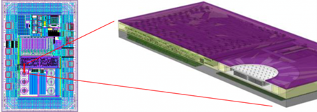
Nanusens describes itself as the only company to have perfected the building of sensors within chips. The micro-electromechanical systems (MEMS) are built using standard chip manufacturing techniques (CMOS) that are used to build the electronic circuits on chips and at the same time as the rest of the chip circuitry. The key impact of their technology is that chips with Nanusens embedded sensors can be made in any of the many CMOS fab in virtually unlimited numbers and with the high yields that are normal in such fabs with the benefits of low unit costs that fab production provides.
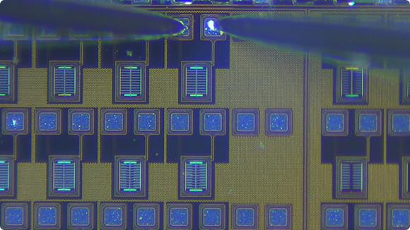
A key innovation by the company is development of a novel control circuit that measures the capacitance changes within the sensor to provide sensor data. Like the sensor itself, this is also a digital IP block so it can be incorporated in the floor plan of the device’s control chip, or ASIC, using standard EDA tools. This pairing for sensors and control circuitry as IP is unique as no other sensor solution can be turned into an IP block and made using standard CMOS techniques within the layers of the chip structure, says the company. Nanusens aims to apply the capabilities to open big markets for its embedded sensors such as smartphones, earbuds, wearables, automotive, medical equipment, aerospace and AIOT, as detailed below. As a result, the company has started a Series A funding round.

Enabling AI to be smarter
AIoT, the fusion of the power of Artificial Intelligence and Internet of Things infrastructure (Artificial Intelligence of Things), is seen as the nirvana market for next generation embedded sensors capable of gathering the data that AIoT needs for mass adoption. Key to its success is having masses of data from sensors that the AI can process. Nanusens sees its technology as disruptive, enabling sensor data to be gathered in a completely new way that will enable mass deployment of AIoT as it slashes the costs and size of sensors to almost nothing.
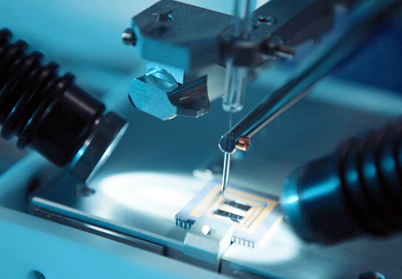
Presently, MEMS sensors are typically manufactured on a tiny sliver of silicon, or die, by a small number of specialist companies with each sensor type being produced on a dedicated production line so it is hard to ramp up production. These are either packaged into the familiar black unit with wire connections to be mounted on a PCB or fixed beside the main chip as a bare die. Both approaches are relatively expensive and large with no current way to reduce costs and size.
Nanusens believes that it has solved both of these problems by creating the sensors directly within the control chip of the device, or ASIC, as the chip is being manufactured. The sensors only take up a virtually insignificant amount of space by being in the chip itself instead of taking up space by being packaged beside it. Also, many different sensors can be built into a chip to make much smarter devices with a negligible increase in costs or space taken up inside the device.
“Being able to include as many sensors as is required within a chip for almost no size or cost penalty is going to revolutionize the design of a whole new generation of smarter AIoT devices,” asserts Montanya. “Until now, IoT has never been able to take off as predicted because the costs of sensors were too great, the size too large, the power consumption too high and the production volumes too constrained. We are the only company to have solved not just one of these barriers but all four by at least an order of magnitude for each one. We enable masses of sensors to be deployed for almost nothing to gather the real world analog data into the IoT network that AI needs to be effective. This is a vital role that will enable the potential of AIoT to be realised. And, naturally, we are building an extensive patent portfolio to protect our unique technology that will empower the AI and IoT revolution that is AIoT.”
Founded in 2014 by Montanya and Dr. Marc Llamas, Nanusens is headquartered in Paignton, Devon, England with research and development offices in Barcelona, Spain and Shenzen, China. For more info, see www.nanusens.com.